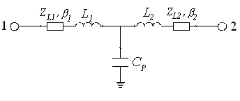
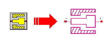
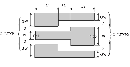
The C_STEP module represents a step in line width and/or line slot of a coplanar line. The dimensions of lines at both sides of a step are defined using data items addressed by C_ LTYP1 and C_TYP2. SL is the step length. L1 and L2 are the lengths of connected coplanar lines at ports.
A negative value for L1 or L2 can be meaningful during the simulation. In such cases, the automated layout generation works incorrectly and the generated layout has to be edited manually. The minimum values for L1 or L2 depend on the metal layer oversizes in the currently selected C_LAYER. In case of DEFAULT foundry, L1 and L2 should be greater than or equal to max(|cond_os|, |cond2_os|).
C_LTYP1 and C_TYP2 must have the same CEN_MET and GND_MET.
A value of SL=0 is not possible, if W1+2S1 £ W2 (or W2+2S2 £ W1).
The difference between the center line widths (W2-W1) has to be an integer multiple of DL. Otherwise the simulator will shift the line at port 1 by a half of grid size (DL/2). In this case the step will become asymmetrical and the user get the message: “(W2-W1)/DL no integer ® asymmetrical step”. Please not that this change is not considered by layout generation. The layout of a step is always symmetrical.
If W1+2S1+2GW1 ¹ W2+2S2+2GW2, there could be an step in the outer contour of the ground strips. In this case, the ground width of the line with smaller value of W+2S+2GW is increased (see layout), so that there is no step in the outer contour of ground planes. This change is considered by the simulation and layout generation.
If W1<W2 and W1+2S1>W2+2S2 (or W2>W1 and W1+2S1<W2+2S2), the step in the inner contour of ground planes is shifted by SL (see layout). This change is considered by the simulation.
If L1 and L2 in selected C_GRID are not set to –1 or –2 (auto sizing), the minimum values for L1 and L2 are:
L1min=max( W1+2*S1+2*GW1, W2+2*S2+2*GW2)
L2min=8*DL{C_GRID}+SL
See notations in chapter 4 (Important Note!) for the correct selection of the C_LTYP1, C_LTYP2.


