[close window] [7 IMST-Utilities]

8 Verification


The IMST developed more than 100 coplanar test circuits, which all consist of passive elements. These structures have been used to verify the simulation models of each coplanar element. The circuit layouts include all layers with under- and oversize information of the Daimler Benz foundry. The layouts were created automatically from a netlist in touchstone format. The design of the total test wafer was made with WaveMaker. Today, the coplanar elements are included into Agilent’s ADS with all possibilities of state of the art circuit design.

This wafer was fabricated at the research center of Daimler Benz in Ulm. The substrate is GaAs with a thickness of 450mm. All test circuits are located twice on the wafer to ensure, that each structure can be evaluated. The simulation of the test circuits has been made with HP-EEsof's Libra. The following substrate parameters are valid for all calculations:

h1=500mm, er1=1., h2=450mm, er2=12.9, h3=1000mm, er3=1.0, k=41S/mm, t1=0.48mm, t2=3mm
DL <= 5mm, gi <= 10-3, ar = 1.8.


Zl / Windication W / mm S/ mm D / mm(=d=GW) ZL_stat/W eeff_stat
50 1 100 75 200 49.8 6.66
50 2 75 56 200 49.3 6.64
50 3 50 37 200 49.3 6.56
50 4 25 19 200 49.5 6.35
40 5 100 35 200 39.7 6.6
60 6 40 57 200 59.5 6.59
70 7 40 103 200 70.1 6.62
50 10 10 100 49.3 5.81


Table 7-1. Geometries of used coplanar waveguides with static values of line impedances and effective permittivities
The main CPW line configurations, which were used in the test circuits, are listed in table 7.1. In the evaluation catalogue the lines are indicated with superscript numbering (e.g. 50W1).
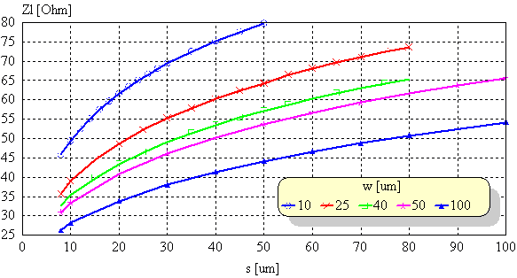


Figure 7-1. Line impedance ZL as a function of the spacing to ground and the line width of coplanar waveguides on GaAs-substrate (450mm thickness)


[close window] [List of Verifications]