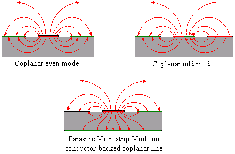
Figure 2-12. Possible propagating modes on coplanar waveguides.
| [close window] | [3 Library Structure] |
| [close window] | [2.10 Effect of Shielding] |
Following instructions will help you to apply the software as efficiently as possible.
- COPLAN for ADS utilizes a numerical field calculation. Therefore, the structures to be calculated are discretized using an automatically generated mesh. The structure dimensions have to fit into the mesh, otherwise the simulator changes the incompatible dimensions (see C_GRID) in order to adapt them to the mesh. As a result, if the changes of the structure dimensions are smaller than 0.25DL (DL is the grid size), these changes are not taken into account. It is therefore recommended to chose grid compatible dimensions for the structure.
- Because of the quasi-static nature of the presented method, dispersion effects are not taken into account. On the other hand, these effects are negligible in case of coplanar structures provided that the structure dimensions are small compared to the substrate height. As an example, the dispersion of effective dielectric constant of a coplanar line with a ground to ground spacing of 625 mm on a 250 mm thick substrate is less than 3% from 1 to 40 GHz.
- The presented method presupposes a pure TEM-wave propagation. This means that the longitudinal field and current components are not considered. As a result, higher order modes are not taken into account. In case of coplanar lines, there are at least two modes which could be excited: even mode and odd mode (see Figure 2-12). Only the even mode is desired and will be assumed in the simulation. The excitation of other modes has to be avoided. The coplanar odd mode may be excited at discontinuities or other asymmetrical constructions and can be suppressed using air bridges.
- If the back side of the substrate is metalized (conductor-backed coplanar line) the coplanar even mode is partially mixed with a so called parasitic microstrip mode. The Figure 2-12 shows the schematic field configuration of this mode. The influence of such microstrip mode on structure characteristics is considered by COPLAN. However, the dispersion effect due to this mode is not taken into account. However, the parasitic microstrip mode has no considerable effect if the ground-to-ground space is smaller than the substrate height.
- Since each element is simulated separately, only the coupling effects within the element itself are considered. The interaction between the elements which are closely connected together can not be taken into account. The user should take care for a proper distance between the elements in order to avoid undesired couplings.

| [close window] | [3 Library Structure] |